Nano in the Negev
January 17, 2014
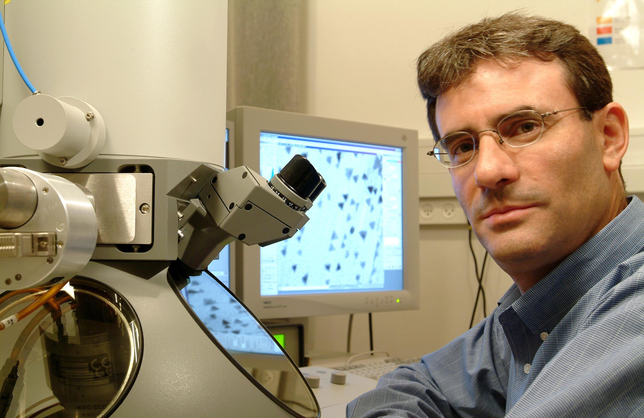
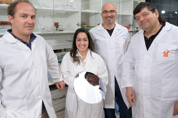
Prof. Yuval Golan, director, Ilse Katz Institute for Nanoscale Science and Technology
TechRepublic — A nanometer is one-billionth of a meter, about the length of 10 hydrogen atoms placed in a row. Or, as Prof. Yuval Golan described it in a recent talk at the Illinois Science and Technology Park, a nanoparticle is roughly one-millionth the size of an ant.
TechRepublic spoke with Prof. Golan, director of Ben-Gurion University’s Ilse Katz Institute for Nanoscale Science and Technology and a member of the University’s Department of Materials Engineering, about the exciting world of nanotechnology.
Excerpts from the interview follow.
TechRepublic: At Ben-Gurion University, what are the areas of nanotech activity related to information technology?
Yuval Golan: We have a startup company in the industrial park that’s working on carbon nanotubes for making supercapacitors, for information storage, for storage of electrical charge, for batteries. There’s a lot going on in that field, a lot. [Elbit Systems is funding this startup.]
Regarding other activity we have that’s related to information technology—there’s one group particularly that’s working on atom chips, making chips from cold atoms, or ion chips. This is directly related to computing.
So for instance if you need a very accurate clock for computing, this is something they’re working on. The researcher’s name is Ron Folman; he is a physics professor working specifically on atom chips, manipulation of atoms with light and temperature for computing applications.
TechRepublic: What do you consider the main applications of nanotechnology?
Yuval Golan: Nanomedicine is huge, including in this building [the Illinois Science and Technology Park]. Another is nanomaterials—for photovoltaics, for thermoelectric materials, for chemical and biological sensors, optical sensors.
All this is making a big impact: homeland security, night vision and energy.
Add to this water technology, nano for water technology. I didn’t mention it in my presentation, but Ben-Gurion University has an institute for water technology [Zuckerberg Institute for Water Technology]. They are working on nanometric membranes, membranes that have very small pores for filtrating water and desalinating water.
Ben-Gurion University is a leader in desalination technology: taking salt water, removing the large amounts of salt and using it for drinking, agriculture and so on. This is the main issue in making special membranes for purifying water, for water treatment of various types. It can be waste, salt water, it can be desalination or regular purifiers.
And the next thing is putting nanoobjects within the membrane. So you don’t just have the small pores—you put in small metal objects or semi-conductor objects that are now actively purifying water. Here we benefit from this very aggressive chemistry associated with nanoparticles that can oxidize organics or decompose poisonous materials, especially organics. We [BGU] have quite a bit of activity in this area.
So I would say medicine, photonics and homeland security, energy, water, and materials in general—these are the five main areas of activity where nanotechnology is already making an impact.
TechRepublic: What is your specific area of research?
Yuval Golan: I am emphasizing the role of interfaces in the application and the preparation of nanomaterials. Think of the device I was describing in my talk [nano night vision glasses] on the layered structure for night vision.
So you have an electron, you have the whole blocking layer, you have the active layer that’s absorbing radiation, the electron blocking layer, the plasmonic enhancing layer, the light-emitting device, and you have a whole lot of interfaces between these layers.
The behavior of these materials and layers will be very much governed by the interfaces. So by controlling the interfaces, orientations, roughness, composition, intermixing—all these are key issues for making a useful device.
I was working at UC Santa Barbara with Jacob Israelachvili, a very famous professor in the area of interfacial science. And I am applying these fundamental studies I learned there to these applied interfaces now for understanding how these materials are talking, or interacting on both sides of the interface.
What we do, first of all we prepare nanomaterials.
Another area of expertise we have is working with conductive polymers. In the future, maybe five years or 10 years, our cell phones and what we have in PCs will definitely be made out of plastic.
There is no doubt about that. It’s going to be polymers—for emitting light, for making processors and transistors, and light-emitting diodes.
All this is going to be made of plastic. We’ve been working on a specific family of conducting polymers, and mostly studying the chemical relationship between the chemical environment in which they are living, and their optical behavior.
This is important for making sensors. If you want, for instance, to sense a given substance, it can be for homeland security, if you want to sense explosives at the airport, or if you want to screen trucks for chemical or biological weapons—all these types of materials can be detected using chemical sensors. And eventually, these will be plastic sensors.
So we are working on this conductive polymer that is very sensitive to the environment. So if you put it in an acidic environment, it will have a different color from a basic environment, and so on.
It’s a pretty interesting materials platform to work on. And what we’re tying to do is to modify it, to put these specially tailor-designed chemical groups for specifically identifying a given substance of interest.
So this in a nutshell is what my research is about.
Read the full article on TechRepublic >>
Stories Like This